Pinout and I/O specification
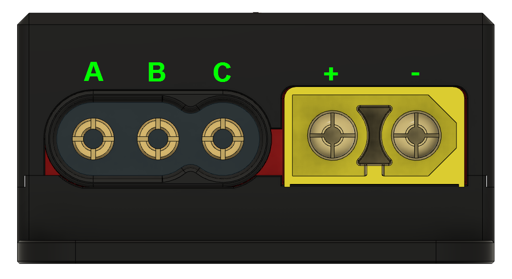
Power connector pinout
Signal connector pinout
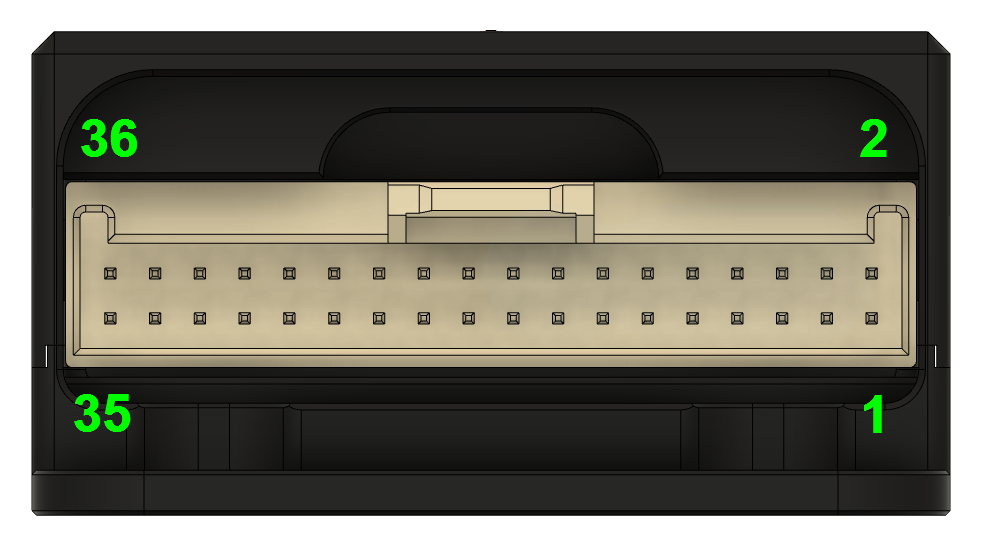
Signal connector pinout table
| Pin number | Pin name | Pin number | Pin name |
|---|---|---|---|
| 1 | CANGND | 2 | CANL |
| 3 | CANH | 4 | HALL+5V |
| 5 | HALLW | 6 | DIN2/DATA |
| 7 | HALLV | 8 | DIN1/CLK |
| 9 | HALLU | 10 | HALLGND |
| 11 | TEMP | 12 | ODIN3+ |
| 13 | ODIN3- | 14 | ODIN4- |
| 15 | ODIN4+ | 16 | DOUT1- |
| 17 | DOUT2+ | 18 | DOUT1+ |
| 19 | POWER | 20 | DOUT2- |
| 21 | POWERGND | 22 | KEY |
| 23 | GPIO GND | 24 | GPIO0 |
| 25 | GPIO +5V | 26 | GPIO1 |
| 27 | GPIO +5V | 28 | USBDP |
| 29 | GPIO GND | 30 | USBDM |
| 31 | USB GND | 32 | USB+5V |
| 33 | COMRXD | 34 | COMTXD |
| 35 | COM+5V/COM+10V | 36 | COMGND |
Pin detailed specifications
Grounding
Function
The controller contains several grounds which are connected to the connectors' pins as shown in the sheme below. Connection between controller heatsink and batt- terminal is also depicted here. Galvanic isolation between GND, GNDIO and ODINs is meant only as functional isolation to prevent communication interfaces from noise. During normal operation voltage between GND, GNDIO and ODINs should be close to zero (several volts maximum).
Scheme
Power circuit
Function
The power circuit provides power to the controller's logic. Power to the internal SMPS (Switched-Mode Power Supply) is controlled by an electronic switch. There are several options for powering on/off, which are described below.
- Constant on
- Activation input
- The device turns on when the battery voltage is applied to the battery terminals and off when removed.
Internal HW configuration for this variant:
- Constant ON - Attached
- One button control - Removed
- Internal fuse - Attached
- The device turns on once battery voltage is applied to the battery terminals and a voltage above 10V is permanently applied to the power pin.
- The device turns off once the voltage is removed from the power pin.
Internal HW configuration for this variant:
- Constant ON - Removed
- One button control - Removed
- Internal fuse - Attached
Scheme
Specification
| Number | Name | Function | Operating range | Maximum rating | Protection |
|---|---|---|---|---|---|
| 22 | KEY | power input for control electronics, connected to BATT+ via 3 A fuse | 0 .. Vbat | 0 .. Vbat | one-time fuse |
| 19 | POWER | power control input (switches controller on/off), min. 8 V for on, max. 0.8 V for off | 0 .. 0.8 V; 10 V .. Vbat | 0 .. Vbat | high impedance |
| 21 | POWERGND | power input ground, internally connected to BATT- | 100 mA |
Voltage between 0.8 V and 8 V on the POWER pin is not allowed, because the controller is in a non-defined state and could be damaged in such a situation.
General purpose analog/digital inputs
Function
Analog inputs are for processing application analog signals (e.g. throttle or brake). Reference potential is shared with the main GND (internally connected to BATT-) Operating range is 0 - 5 V.
Scheme
Specification
| Number | Name | Function | Operating range | Maximum rating |
|---|---|---|---|---|
| 23 | GPIO GND | ground for gpios, connected internally to BATT- | 50 mA | |
| 29 | GPIO GND | ground for gpios, connected internally to BATT- | 50 mA | |
| 25 | GPIO +5V | 5 V output for gpio | 5 V / 50 mA* | |
| 27 | GPIO +5V | 5 V output for gpio | 5 V / 50 mA* | |
| 24 | GPIO0 | Input, max. 2% measurement error | 0 .. 5 V | 0 V .. 6.6 V |
| 26 | GPIO1 | Input, max. 2% measurement error | 0 .. 5 V | 0 V .. 6.6 V |
Note *: see Internal supply parameters
Optically isolated digital inputs
Function
Digital inputs are for processing application digital signals (e.g. buttons or PPM signals). The operating range is 10 V - 60 V for logic 1 and 0 V - 3 V for logic 0. ODIN+ pin is tolerant to full battery voltage. In the default configuration, they are completely isolated from other controllers' circuits (this is not true if the pull-up or pull-down jumper is used). This input can also measure pulse length (PPM).
Scheme
Specification
| Number | Name | Function | Operating range | Maximum rating | protection |
|---|---|---|---|---|---|
| 12 | ODIN3+ | positive input of (opto)isolated DIN3 (-> ODIN3) | 0 .. 60 V | 0 .. 80 V, 15mA | galvanic isolation |
| 13 | ODIN3- | negative input of (opto)isolated DIN3 (-> ODIN3) | 0 .. 60 V | 0 .. 80 V, 15mA | galvanic isolation |
| 15 | ODIN4+ | positive input of (opto)isolated DIN4 (-> ODIN4) | 0 .. 60 V | 0 .. 80 V, 15mA | galvanic isolation |
| 14 | ODIN4- | negative input of (opto)isolated DIN4 (-> ODIN4) | 0 .. 60 V | 0 .. 80 V, 15mA | galvanic isolation |
Note 1: pulse length measurement range: 800 us - 2200 us for 0 V / 5 V signal, error max. +/-25 us
Note 2: digital input: max. 3 V for LOW, min. 10 V for HIGH
Note 3: when ODIN is configured as floating, it is galvanically isolated from BATT-, from CANGND, COMGND and from the other ODIN input
Note 4: when ODIN is configured as pull-up, ODIN+ is connected internally to GPIO+5V
Note 5: when ODIN is configured as pull-down, ODIN- is connected internally to BATT- (HALLGND, GPIO, POWERGND)
Non-isolated digital inputs
Function
Non-isolated digital inputs are for processing application digital signals (e.g. buttons). These inputs are part of the MSENS circuit and are available only for the MSENS "a" assembly variant. The reference potential is common with the controller's power GND.
Scheme
Specification
| Number | Name | Function | Operating range | Maximum rating | Protection |
|---|---|---|---|---|---|
| 8 | DIN1/CLK | DIN1 (max. 3 V for LOW, min 8 V for HIGH), EXC+, CLK+ | 0 .. 60 V* | 0 .. VBat* | high impedance |
| 6 | DIN2/DATA | DIN2 (max. 3 V for LOW, min 8 V for HIGH), EXC-, DATA+ | 0 .. 60 V* | 0 .. VBat* | high impedance |
Note *: valid for msens assembly variant "a"
Digital open-drain outputs
Function
Digital open-drain outputs, capable of driving an inductive load with a maximum current load capacity of 500 mA. There is no inbuilt overcurrent or overload protection (except the fuse on the KEY pin) and it is necessary to keep the current below the maximal current specifications. Inductive load should be connected between corresponding DOUT+ and DOUT- pins.
Scheme
Specification
| Number | Name | Function | Maximum rating | Protection |
|---|---|---|---|---|
| 16 | DOUT1- | Open-drain digital output, capable of inductive load switching, when connected between DOUT+ and DOUT- | 500 mA | |
| 18 | DOUT1+ | Positive output for DOUT, internally connected to pin 22 KEY and pin 17 DOUT2+ | 500 mA | one-time fuse |
| 20 | DOUT2- | Open-drain digital output, capable of inductive load switching, when connected between DOUT+ and DOUT- | 500 mA | |
| 17 | DOUT2+ | Positive output for DOUT, internally connected to pin 22 KEY and pin 18 DOUT1+. | 500 mA | one-time fuse |
Motor position sensor
- Variant - a
- Variant - r
- Variant - e
Function
Motor position sensor variant "a" can process 3 hall sensors or sin/cos position sensors and 2 inputs that can be used as non-isolated digital inputs (more information about DINs here).
HALLV/SIN and HALLU/COS inputs have combined functions. These inputs can process digital as well as analog signals, which means that can be used for sensing two state Halls and also sine and cosine signals. HALLW/COM can be used only for sensing digital signals. All these inputs work in the range from 0 to 5 V. Reference potential is shared with the main GND (internally connected to BATT-).
UVW hall sensors connection
| Pin number | Pin name | Function |
|---|---|---|
| 10 | HALLGND | Sensor ground |
| 4 | HALL+5V | Sensor +5V supply |
| 9 | HALLU | Hall U digital input |
| 7 | HALLV | Hall V digital input |
| 9 | HALLW | Hall W digital input |
Sin-Cos sensor connection
| Pin number | Pin name | Function |
|---|---|---|
| 10 | HALLGND | Sensor ground |
| 4 | HALL+5V | Sensor +5V supply |
| 9 | HALLU | Cosine analog input |
| 7 | HALLV | Sine analog input |
Scheme
Resolver connection
| Pin number | Pin name | Function |
|---|---|---|
| 9 | HALLU | Cosine+ analog input |
| 7 | HALLV | Sine+ analog input |
| 5 | HALLW | Sine- and Cosine- common analog input |
| 8 | DIN1/CLK | Resolver excitation+ output |
| 6 | DIN2/DATA | Resolver excitation- output |
Digital sensor connection (SSI, BiSS)
| Pin number | Pin name | Function |
|---|---|---|
| 10 | HALLGND | Sensor ground |
| 4 | HALL+5V | Sensor +5V supply |
| 8 | DIN1/CLK | CLOCK digital output |
| 6 | DIN2/DATA | DATA digital input |
The CLOCK and DATA are single-ended signals, not differential. For diferential signal:
- Add 470ohm resistor between positive and negative signal lines on the DATA output.
- Negative CLOCK signal leave unconnected.
For more details, please check datasheet of your sensor and its recommended connection scheme.
Sin-Cos sensor connection
| Pin number | Pin name | Function |
|---|---|---|
| 10 | HALLGND | Sensor ground |
| 4 | HALL+5V | Sensor +5V supply |
| 9 | HALLU | Cosine analog input |
| 7 | HALLV | Sine analog input |
Using Sin-Cos sensor with variant "r" is not typical usecase, but it is possible.
Scheme
Variant development in progress. Contact siliXcon R&D for more information.
This variant is meant for economic applications, with support for incremental encoders only. It does not support Sin-Cos sensors or resolvers.
Specification
| Number | Name | Function | Operating range | Maximum rating | Protection |
|---|---|---|---|---|---|
| 10 | HALLGND | ground for msens inputs, TEMP input and supply, connected internally to BATT- | 100 mA | ||
| 4 | HALL+5V | 5 V power supply output for msens | 5 V / 100 mA ** | ||
| 9 | HALLU | HALLU (max. 1 V for LOW, min 4 V for HIGH), COS | 0 .. 5 V | 0 .. 12 V* | high impedance |
| 7 | HALLV | HALLV (max. 1 V for LOW, min 4 V for HIGH), SIN, ENCB+ | 0 .. 5 V | 0 .. 12 V* | high impedance |
| 5 | HALLW | HALLW (max. 1 V for LOW, min 4 V for HIGH), CLK- | 0 .. 5 V | 0 .. 12 V* | high impedance |
Note *: valid for msens assembly variant "a"
Note **: see Internal supply parameters
Motor temperature sensor
Function
The motor temperature sensor circuit is designed to work with resistance ranging from 100 Ohms up to 10 kOhms. The TEMP pin has an internal pull-up connected to 5 V, providing power for the motor temperature sensor.
Scheme
Specification
| Number | Name | Function | Operating range | Maximum rating | Protection |
|---|---|---|---|---|---|
| 10 | HALLGND | ground for msens inputs, TEMP input and supply, connected internally to BATT- | 100 mA | ||
| 11 | TEMP | motor temperature sensor input, max. 5% error | 0 .. 5 V | 0 .. 12 V | high impedance |
CAN communication interface
Function
CAN communication interface is galvanically isolated from the main power GND. 120 Ohm terminator can be activated via an internal jumper on request.
Scheme
Specification
| Number | Name | Function | Operating range | Maximum rating | Protection |
|---|---|---|---|---|---|
| 1 | CANGND | CAN communication ground, isolated from BATT-, connected internally to COMGND | 50 mA | galvanic isolation | |
| 2 | CANL | CAN communication, isolated from BATT- | 0 - 5 V | +/- 70 V* | galvanic isolation |
| 3 | CANH | CAN communication, isolated from BATT- | 0 - 5 V | +/- 70 V* | galvanic isolation |
Note *: +/- 70V between CANL and CANH only when CAN_GND is connected to neither of these two pins. Other possibilities have not been tested. Contact siliXcon for more information.
Isolated USART communication interface
Function
UARTcom communication interface is galvanically isolated from the main power GND. RX and TX have an operating range of 0 – 5 V. UART interface has also a dedicated 5 V power source for external accessories.
Scheme
Specification
| Number | Name | Function | Operating range | Maximum rating | Protection |
|---|---|---|---|---|---|
| 36 | COMGND | USART communication ground, isolated from BATT-, connected internally to CANGND | 50 mA | galvanic isolation | |
| 35 | COM+5V/COM+10V | 5 V USART communication supply (10 V on request ***) | 5 V / 50 mA ** | galvanic isolation | |
| 34 | COMTXD | USART communication, isolated from BATT- | 0 - 5 V | 0 V .. 5.5 V | galvanic isolation |
| 33 | COMRXD | USART communication, isolated from BATT- | 0 - 5 V | 0 V .. 5.5 V | galvanic isolation |
Note : see Internal supply parameters
Note *: 10 V output is not stabilized, output voltage could vary from 5 V to
13 V, depending on battery voltage and power supply load. Contact siliXcon
for more information.
USB communicaton interface
Function
USB communication interface is there only for parametrization purposes. This interface is not galvanically isolated from the power GND.
Do not use USB communication with a PC once the motor is driven. There is a risk of damage to the controller or the PC.
Scheme
Specification
| Number | Name | Function | Operating range | Maximum rating |
|---|---|---|---|---|
| 31 | USB GND | USB ground | 100 mA | |
| 32 | USB+5V | 5V input for powering via USB | 5 V | 5.5 V |
| 28 | USBDP | USB data+ | 0 - 3.3 V | 0 V .. 3.6 V |
| 30 | USBDM | USB data- | 0 - 3.3 V | 0 V .. 3.6 V |
PWM/PPM capture input pins channel mapping
| Pin | Reference | CMIO Channel | Availability |
|---|---|---|---|
| ODIN4 | differential | ch1 | always |
| ODIN3 | differential | ch2 (default) | always |
| USARTCOM RX | COMGND (isolated) | ch4 | USART COM must be disabled (msgconf 1 0) |
Internal supply parameters
Maximum allowed currents from individual branches
| Supply branch | Outputs | Maximum branch current |
|---|---|---|
| Unisolated | pin 4 - HALL+5V, pins 25, 27 - GPIO+5V | 150 mA |
| Isolated | pin 35 - COM+5V/COM+10V | 50 mA |
Maximum allowed total current
| Controller variant | Used supply | Maximum total current |
|---|---|---|
| all d variants (05dxa0810, 06dxa0810 ...) | LM5017 | 200 mA |
| all k variants (05kxa0810, 06kxa0810 ...) | LM5008 | 150 mA |