Pinout and I/O specification
Power connector pinout
Power connection is done by M6 terminals according to this chapter
Signal connector pinout
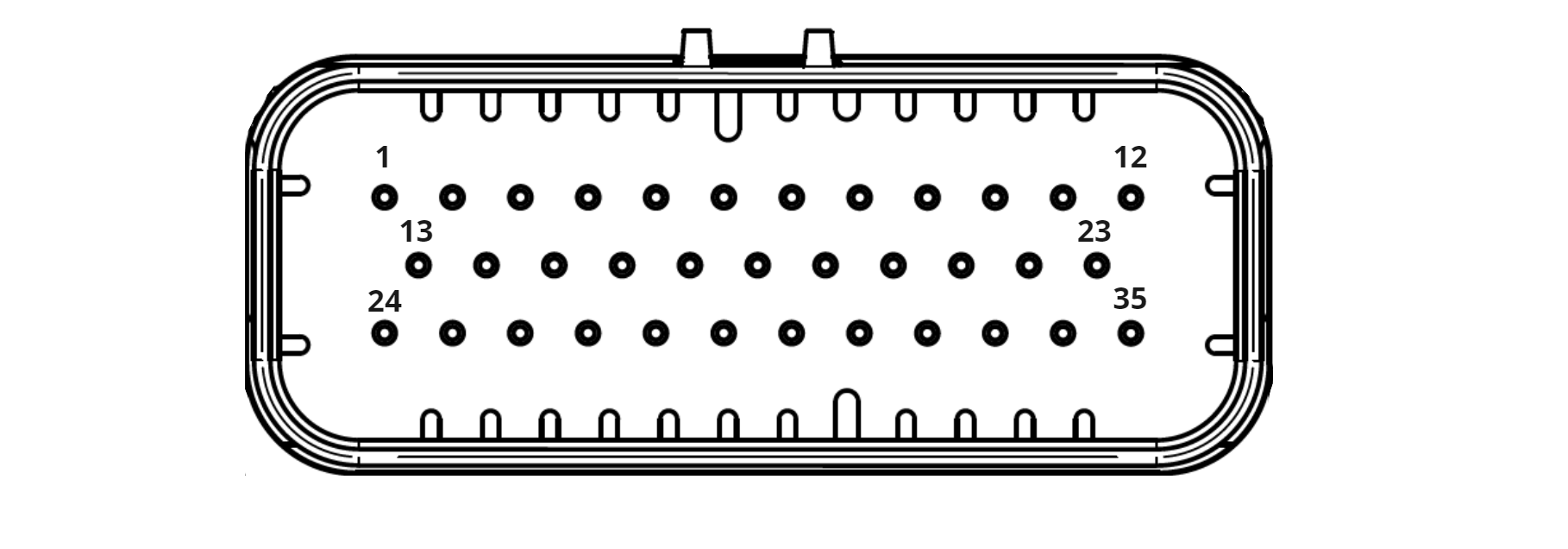
Signal connector pinout table
| Pin number | Pin name | Pin number | Pin name |
|---|---|---|---|
| 1 | KEY1 | 2 | CANTERM |
| 3 | CONT1- | 4 | CONT1+ |
| 5 | HALLU/COS | 6 | GND |
| 7 | CONT2- | 8 | CONT2+ |
| 9 | GPIO3 | 10 | IOGND |
| 11 | CONT3- * | 12 | CONT3+ * |
| 13 | CANH | 14 | ENCA/CLK |
| 15 | HALL_GND | 16 | RXD |
| 17 | HALLV/SIN | 18 | ADIN1 |
| 19 | ADIN3 | 20 | POWER |
| 21 | GPIO4 | 22 | GPIO0 |
| 23 | GPIO1 | 24 | CANL |
| 25 | ENCB/DATA | 26 | HALL+5V |
| 27 | TXD | 28 | IO+10V |
| 29 | HALLW/COM | 30 | ADIN2 |
| 31 | ADIN4 | 32 | GPIO2 |
| 33 | TEMP | 34 | IO+3V |
| 35 | IO+5V |
Note *: Contactor 3 is not available in the *AFFGG* (e.g. esc3-sl1k_48exa1580-400_AFFGG-600BB). Pins 11 CONT3- and 12 CONT3+ are not internally connected in this variant.
USB-B connector pinout

USB-B connector pinout table
| Pin number | Pin name |
|---|---|
| 1 | USB5V |
| 2 | USBDM |
| 3 | USBDP |
| 4 | USBGND |
Pin detailed specifications
Controller grounds connection
Function
The controller contains several grounds which are connected to the connectors' pins as shown in the scheme below. Connection between controller heatsink and batt- terminal is also depicted here. Galvanic isolation between GND and GNDIO is meant only as functional isolation to prevent signal inputs and communication interfaces from noise. During normal operation voltage between GND and GNDIO should be close to zero (several volts maximum).
Scheme
Power circuit
Function
The power circuit provides power to the controller's logic. Power to the internal SMPS (Switched-Mode Power Supply) is controlled by an electronic switch. There are several options for powering on/off, which are described below.
- Constant on
- Flip-flop
- Flip-flop with precharge
- Activation input
- Activation input with precharge
- The device turns on when the battery voltage is applied to the battery terminals and off when removed.
Internal HW configuration for this variant:
- Key resistor - Attached
- Flip-flop - Removed
- Internal fuse - Attached
- The device turns on once the battery voltage is applied to the battery terminals and a voltage above 10V is applied to the power pin. The latching function of the flip-flop ensures that it remains turned on even when the voltage on the power pin is disconnected.
- The device turns off once a voltage below 1V is applied to the power pin (usually done by connecting the pin to the GND).
- It is also possible to turn off the device by FW.
Internal HW configuration for this variant:
- Key resistor - Removed
- Flip-flop - Attached
- Internal fuse - Attached
- The device starts precharging once a voltage above 10V is applied to the power pin. After the precharge is completed the main contactor is switched on and the battery voltage is applied to the battery terminals and controller is powered up. The latching function of the flip-flop ensures that it remains in this state even when the voltage on the power pin is disconnected.
- The device turns off once a voltage below 1V is applied to the power pin (usually done by connecting the pin to the GND).
- It is also possible to turn off the device by FW.
The device needs to be equipped with precharge Power Feature for this powering variant
Internal HW configuration for this variant:
- Key resistor - Removed
- Flip-flop - Attached
- Internal fuse - Removed
- The device turns on once battery voltage is applied to the battery terminals and a voltage above 10V is permanently applied to the power pin.
- The device turns off once the voltage is removed from the power pin.
Internal HW configuration for this variant:
- Key resistor - Removed
- Flip-flop - Removed
- Internal fuse - Attached
- The device starts precharging once a voltage above 10V is applied to the power pin. After the precharge is completed the main contactor is switched on and the battery voltage is applied to the battery terminals and controller is powered up.
- The device turns off once the voltage is removed from the power pin.
The device needs to be equipped with precharge Power Feature for this powering variant
Internal HW configuration for this variant:
Jumpers configuration for this variant:
- Key resistor - Removed
- Flip-flop - Removed
- Internal fuse - Removed
Internal fuse can not be used for middle voltage edition of the controller. This effectivelly means that from powering variants listed above, only these with precharge can be used for the middle voltage edition of the controller.
Specification
| Number | Name | Function | Operating range | Maximum rating |
|---|---|---|---|---|
| 1 | KEY1 | power input for control electronics | 0 .. Vbat | 0 .. Vbat |
| 20 | POWER | power control input (switches controller on/off) | 0 .. Vbat | 0 .. Vbat |
| 6 | GND | power input ground | 500 mA |
General purpose analog/digital inputs
Function
These inputs can be used for processing analog and digital voltage levels. These inputs are galvanically isolated from the Power GND, motor sensor GND and external UART GND. The controller offers several isolated power sources. These can be used as a power source for the external components (e.g. throttle). Pull-up and pull-down resistors on all inputs can be set individually by FW parameters.
Scheme
Specification
| Number | Name | Function | Operating range | Maximum rating | Protection |
|---|---|---|---|---|---|
| 10 | IOGND | GPIO ground, isolated from BATT- | 100 mA | galvanic isolation | |
| 22 | GPIO0 | Input, isolated from BATT- | 0 .. 10 V * | 0 .. 12 V | galvanic isolation + high impedance + 12 TVS + 100 mA PTC |
| 23 | GPIO1 | Input, isolated from BATT- | 0 .. 10 V * | 0 .. 12 V | galvanic isolation + high impedance + 12 TVS + 100 mA PTC |
| 32 | GPIO2 | Input, isolated from BATT- | 0 .. 10 V * | 0 .. 12 V | galvanic isolation + high impedance + 12 TVS + 100 mA PTC |
| 9 | GPIO3 | Input, isolated from BATT- | 0 .. 10 V * | 0 .. 12 V | galvanic isolation + high impedance + 12 TVS + 100 mA PTC |
| 21 | GPIO4 | Input, isolated from BATT- | 0 .. 10 V * | 0 .. 12 V | galvanic isolation + high impedance + 12 TVS + 100 mA PTC |
| 21 | GPIO4*** | Input, isolated from BATT- | 0 .. 5 V * | 0 .. 5.5 V | galvanic isolation + 12 TVS + 100 mA PTC |
| 34 | IO+3V | 3 V power supply output for GPIO, isolated from BATT- | 3 V / 100 mA ** | galvanic isolation + 12 TVS + 100 mA PTC | |
| 35 | IO+5V | 5 V power supply output for GPIO, isolated from BATT- | 5 V / 100 mA ** | galvanic isolation + 12 TVS + 100 mA PTC | |
| 28 | IO+10V | 10 V power supply output for GPIO, isolated from BATT- | 10 V / 100 mA ** | galvanic isolation + 12 TVS + 100 mA PTC |
Note *: range could be extended by FW configuration (pull-up and pull-down resistors)
Note **: see Internal supply parameters
Note ***: valid for communication variant "p"(GPIO4 modified to accept PWM/PPM input)
Non-isolated Analog/Digital inputs
Function
4 ADIN inputs are for processing application analog/digital signals (e.g. buttons or analog voltage). The operating range is 0 V - Vbat. PUPD can be connected (by FW parameter) to KEY (pin 1) or to GND (pin6) acting then as pull-up or pull-down. Also, the threshold for logic 0 and 1 (in the case of digital inputs) can be set by an FW parameter.
- Standard / Raptor Fan edition
- Middle Voltage / Raptor Fan edition
Scheme
Specification
| Number | Name | Function | Operating range | Maximum rating | protection |
|---|---|---|---|---|---|
| 18 | ADIN1 | Non-isolated analog/digital input | 0 .. Vbat | 0 .. 84 V, 15mA | high impedance |
| 30 | ADIN2 | Non-isolated analog/digital input | 0 .. Vbat | 0 .. 84 V, 15mA | high impedance |
| 19 | ADIN3 | Non-isolated analog/digital input | 0 .. Vbat | 0 .. 84 V, 15mA | high impedance |
| 31 | ADIN4 | Non-isolated analog/digital input | 0 .. Vbat | 0 .. 84 V, 15mA | high impedance |
Scheme
Specification
| Number | Name | Function | Operating range | Maximum rating | protection |
|---|---|---|---|---|---|
| 18 | ADIN1 | Non-isolated analog/digital input | 0 .. Vbat | 0 .. 118 V, 15mA | high impedance |
| 30 | ADIN2 | Non-isolated analog/digital input | 0 .. Vbat | 0 .. 118 V, 15mA | high impedance |
| 19 | ADIN3 | Non-isolated analog/digital input | 0 .. Vbat | 0 .. 118 V, 15mA | high impedance |
| 31 | ADIN4 | Non-isolated analog/digital input | 0 .. Vbat | 0 .. 118 V, 15mA | high impedance |
Digital open-drain outputs
Function
SL controller has a total of 3* digital open-drain outputs, capable of driving an inductive load with a maximum current load capacity of 500 mA each. This output has inbuilt overcurrent and shortcut protection (feedback from current measurement and internal 750 mA reversible fuse). The output voltage can be controlled by PWM. These digital outputs are usually used for driving a battery contactor or external accessories (pumps, fans, etc.).
Scheme
Specification
| Number | Name | Function | Maximum rating | Protection |
|---|---|---|---|---|
| 3 | CONT1- | contactor negative terminal, PWM switched to GND | 500 mA | overcurrent protection |
| 7 | CONT2- | contactor negative terminal, PWM switched to GND | 500 mA | overcurrent protection |
| 11 | CONT3-* | contactor negative terminal, PWM switched to GND | 500 mA | overcurrent protection |
| 4 | CONT1+ | contactor positive terminal | 500 mA | Reversible 750mA fuse |
| 8 | CONT2+ | contactor positive terminal | 500 mA | Reversible 750mA fuse |
| 12 | CONT3+* | contactor positive terminal | 500 mA | Reversible 750mA fuse |
Note *: Contactor 3 is not available in the *AFFGG* (e.g. esc3-sl1k_48exa1580-400_AFFGG-600BB). Pins 11 CONT3- and 12 CONT3+ are not internally connected in this variant.
Motor position sensor
- Variant - a
- variant - r
Function
If you have a differential sensor interface, leave the negative ends unconnected. SiliXcon controllers employ an advanced synchronous sampling technique, and differential connection is optional. Please contact us for other options. The SL controller can be fitted with a fully differential input on demand.
Motor position sensor variant "a" can process 3 hall sensors or sin/cos position sensors and 2 inputs that can be used as non-isolated digital inputs (more information about DINs here).
HALLV/SIN and HALLU/COS inputs have combined functions. These inputs can process digital as well as analog signals, which means that can be used for sensing two state Halls and also sine and cosine signals. HALLW/COM can be used only for sensing digital signals. All these inputs work in the range from 0 to 5 V. Reference potential is shared with the main GND (internally connected to BATT-).
UVW hall sensors connection
| Pin number | Pin name | Function |
|---|---|---|
| 15 | HALL_GND | Sensor ground |
| 26 | HALL+5V | Sensor +5V supply |
| 5 | HALLU/COS | Hall U digital input |
| 17 | HALLV/SIN | Hall V digital input |
| 29 | HALLW/COM | Hall W digital input |
Sin-Cos sensor connection
| Pin number | Pin name | Function |
|---|---|---|
| 15 | HAL_LGND | Sensor ground |
| 26 | HALL+5V | Sensor +5V supply |
| 5 | HALLU/COS | Cosine analog input |
| 17 | HALLV/SIN | Sine analog input |
Incremental encoder connection (ABZ)
| Pin number | Pin name | Function |
|---|---|---|
| 15 | HALLGND | Sensor ground |
| 26 | HALL+5V | Sensor +5V supply |
| 14 | ENCA/CLK | ENCA digital input |
| 25 | ENCB/DATA | ENCB digital input |
| 29 | HALLW/COM | ENCREF+ (Z) digital input (optional) |
| 17 | HALLV/SIN | PWM homing input (optional) |
Scheme
Function
Motor position sensor variant "r" can excite the motor resolver and process signals from it.
HALLV/SIN and HALLU/COS inputs can process analog signals and are used for sensing sin and cos outputs from the resolver. HALLW/COM is used as common ground for the sin and cos outputs. Excitation for the resolver is taken from ENCA/CLK and ENCB/DATA. The reference potential is shared with the main GND (internally connected to BATT-).
Resolver connection
| Pin number | Pin name | Function |
|---|---|---|
| 5 | HALLU/COS | Cosine+ analog input |
| 17 | HALLV/SIN | Sine+ analog input |
| 29 | HALLW/COM | Sine- and Cosine- common analog input |
| 14 | ENCA/CLK | Resolver excitation+ output |
| 25 | ENCB/DATA | Resolver excitation- output |
Digital sensor connection (SSI, BiSS)
| Pin number | Pin name | Function |
|---|---|---|
| 15 | HALL_GND | Sensor ground |
| 26 | HALL+5V | Sensor +5V supply |
| 14 | ENCA/CLK | CLOCK digital output |
| 25 | ENCB/DATA | DATA digital input |
Scheme
Specification
| Number | Name | Function | Operating range | Maximum rating | Protection |
|---|---|---|---|---|---|
| 15 | HALLGND | ground for msens inputs and supply | 100 mA | slow blow fuse | |
| 26 | HALL+5V | 5 V power supply output for msens | 5 V / 100 mA* | overcurrent and shortcut | |
| 5 | HALLU/COS | HALLU (max. 1 V for LOW, min 4 V for HIGH), COS | 0 .. 5 V | 0 .. 12 V | high impedance, 100mA PTC, 12V TVS |
| 17 | HALLV/SIN | HALLV (max. 1 V for LOW, min 4 V for HIGH), SIN | 0 .. 5 V | 0 .. 12 V | high impedance, 100mA PTC, 12V TVS |
| 29 | HALLW/COM | HALLW (max. 1 V for LOW, min 4 V for HIGH), COM | 0 .. 5 V | 0 .. 12 V | high impedance, 100mA PTC, 12V TVS |
| 14 | ENCA/CLK | EXC+ | 0 .. 5 V | 0 .. 12 V | high impedance, 100mA PTC, 12V TVS |
| 25 | ENCB/DATA | EXC- | 0 .. 5 V | 0 .. 12 V | high impedance, 100mA PTC, 12V TVS |
Note **: see Internal supply parameters
Motor temperature sensor
Function
The motor temperature sensor circuit is designed to work with resistance ranging from 100 Ohms up to 10 kOhms. The TEMP pin has an internal pull-up connected to 5 V, providing power for the motor temperature sensor.
Scheme
Specification
| Number | Name | Function | Operating range | Maximum rating | Protection |
|---|---|---|---|---|---|
| 15 | HALLGND | MSENS GND | 100 mA | slowblow fuse | |
| 33 | TEMP | motor temperature sensor input | 0 .. 5 V | 0 .. 12 V | high impedance, 100mA PTC, 12V TVS |
CAN communication interface
Function
CAN communication interface is galvanically isolated from the main power GND. 120 Ohm terminator can be activated via an internal jumper on request or by installing a jumper on the pins closer to the main signal connector. Position of the jumper can be found here. Each pin is protected by 100 mA reversible fuse. CANL and CANH pins have also 12V TVS overvoltage protection.
Scheme
Specification
| Number | Name | Function | Operating range | Maximum rating | Protection |
|---|---|---|---|---|---|
| 2 | CANTERM | 120 Ohm terminator output | 0 - 5 V | galvanic isolation, 100 mA PTC | |
| 13 | CANH | CAN communication, isolated from BATT- | 0 - 5 V | +/- 70 V* | galvanic isolation, 100 mA PTC, 12 V TVS |
| 24 | CANL | CAN communication, isolated from BATT- | 0 - 5 V | +/- 70 V* | galvanic isolation, 100 mA PTC, 12 V TVS |
| 10 | IOGND | IO common ground, isolated from BATT- | 100 mA | galvanic isolation |
Note *: +/- 70V between CANL and CANH only when CAN_GND is connected to neither of these two pins. Other possibilities have not been tested. Contact siliXcon for more information.
Isolated USART communication interface
Function
UARTcom communication interface is galvanically isolated from the main power GND. RX and TX have an operating range of 0 – 5 V. UART interface has also a dedicated 5 V power source for external accessories.
Scheme
Specification
| Number | Name | Function | Operating range | Maximum rating | Protection |
|---|---|---|---|---|---|
| 16 | RXD | USART communication, isolated from BATT- | 0 - 5 V | 0 V .. 5.5 V | galvanic isolation, 100 mA PTC, 12 V TVS |
| 27 | TXD | USART communication, isolated from BATT- | 0 - 5 V | 0 V .. 5.5 V | galvanic isolation, 100 mA PTC, 12 V TVS |
| 35 | IO+5V_OUT | Isolated power +5 V supply | 100 mA* | galvanic isolation, 100 mA PTC, 12 V TVS | |
| 10 | IOGND | IO common ground, isolated from BATT- | 100 mA | galvanic isolation |
Note *: see Internal supply parameters
USB communicaton interface
Function
USB communication interface is there only for parametrization purposes. This interface is not galvanically isolated from the power GND.
Do not use USB communication with a PC once the motor is driven. There is a risk of damage to the controller or the PC.
Scheme
Specification
| Number | Name | Function | Operating range | Maximum rating |
|---|---|---|---|---|
| 1 | VBUS | 5 V power supply input | 5 V | 5.5 V |
| 4 | USBGND | USB ground | 100 mA | |
| 3 | D+ | Data + | 3.3 V | 3.6 V |
| 2 | D- | Data - | 3.3 V | 3.6 V |
PWM/PPM capture input pins channel mapping
| Pin | Reference | CMIO Channel | Availability |
|---|---|---|---|
| MSENS ENCB | HALLGND (non-isolated, ultra fast) | ch1 (default) | pin must not be used by MSENS |
| MSENS ENCA | HALLGND (non-isolated, ultra fast) | ch2 | pin must not be used by MSENS |
| USARTCOM RX | COMGND (isolated) | ch2 | USART COM must be disabled (set msgconf 1 0) |
| GPIO4 | IOGND (isolated) | ch5 | connectivity variant 'p' required, set ioconf4 to 3 |
Internal supply parameters
| Supply branch | Outputs | Maximum branch current |
|---|---|---|
| Unisolated | pin 26 - +5V_MSENS | 100 mA |
| Isolated | pin 28 - IO+10V, pin 35 - IO+5V, pin 34 - IO+5V | 50 mA * |
Note *: Minimum supply voltage to achieve this parameter is 32 V. If load on unisolated branch is at least 50 mA, minimum supply voltage can be as low as 22 V.
Maximum allowed total current
| Controller power feature variant | Used supply | Maximum total current |
|---|---|---|
| e | LM5008 | 150 mA |